RF Drone Detection Prototype
RF front-end prototype exploring detection of signals associated with common drone communication bands
For a design competition, I developed the electrical architecture for a compact receiver concept that could observe RF energy in frequency regions commonly used by drone communication links. I designed the path from the antenna through RF gain and filtering to logarithmic power detection and an MCU-readable output, then translated the system into a custom PCB.
My scope: electrical architecture, component selection, schematic capture, and the first PCB layout iteration. The project was a prototype exploration—not a validated drone-identification system or production receiver.
- Project stage
- Competition prototype
- Primary focus
- RF + analog hardware
- Layout goal
- Designed toward 50 Ω
RF signal chain
The receiver converts high-frequency energy at the antenna into a practical analog measurement for embedded electronics.
The design goal was to turn a small, high-frequency antenna signal into a low-frequency measurement that a conventional microcontroller could read. Because RF behaviour depends on interconnect geometry and return paths, the signal could not be treated like an ordinary low-frequency analog input.
The gain stage raises the incoming signal level, the filters limit which parts of the spectrum reach the detector, and the AD8318 converts RF input level into an analog voltage. The MCU can then sample that voltage instead of attempting to digitize a multi-gigahertz waveform directly.
- RF interfaces
- U.FL antenna connections
- Detection output
- Low-frequency analog voltage
- Supporting systems
- 5 V / 3.3 V rails + radio module
My first RF PCB layout
This was my first time experimenting with controlled-impedance and impedance-matched RF traces on a PCB. I designed toward the 50 Ω interconnect convention used by the selected RF components, without claiming that the finished geometry was verified with a VNA.
Key learningOne of the biggest changes from my previous PCB work was realizing that at RF frequencies, a PCB trace is no longer just a wire. Its geometry and return path become part of the circuit.
The layout exercise changed how I thought about a connection on a board. Trace width, stackup, dielectric thickness, copper geometry, and the nearby ground reference all influence characteristic impedance. Pads, connectors, branches, and routing changes can add discontinuities, while longer routes make placement decisions increasingly important as frequency rises.
- 01Design RF interconnects around a target geometry and board stackup
- 02Keep a continuous ground reference beneath the RF path
- 03Use short, direct connections between RF components
- 04Reduce abrupt branches and routing discontinuities
- 05Separate sensitive RF sections from switching power where practical
- 06Place local decoupling close to the devices it supports
Antenna and gain stage
The receiver begins at a U.FL antenna interface. The coupled RF signal enters a PGA-103+ gain stage, followed by its bias and support network before continuing into the filtering section.
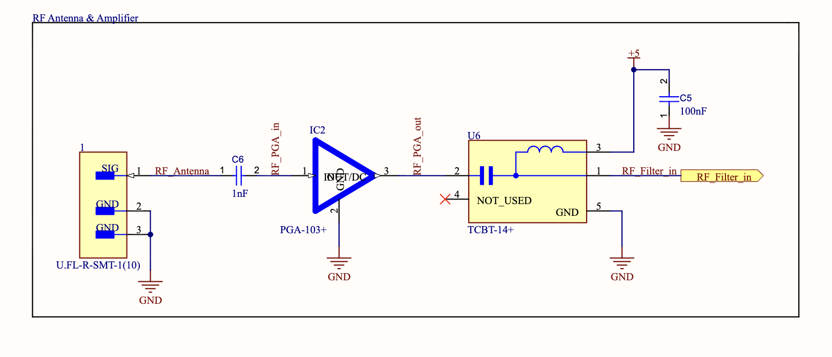
This portion of the schematic established the transition from the external RF connection into the on-board signal path. Placement and routing around the connector, coupling component, amplifier, and grounded support components were therefore part of the electrical design—not just a packaging step.
- U.FL antenna input
- RF / AC coupling
- PGA-103+ gain stage
- Bias and local support circuitry
Filtering and RF detection
Mini-Circuits filter components were placed ahead of an AD8318 logarithmic RF detector. The network was intended to make the receiver more selective to frequency regions of interest rather than allowing a broadband detector to respond equally to every nearby RF source.
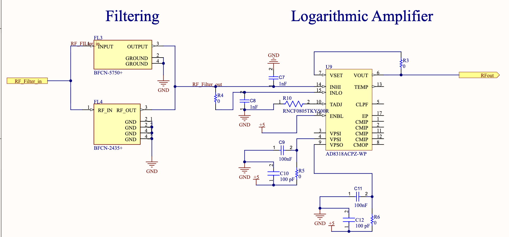
The AD8318 converts RF input level into an analog output voltage suitable for the MCU interface. The schematic defines the intended filtering and detection architecture; it does not establish measured filter response, calibrated detector accuracy, or a validated drone-detection range.
Power architecture
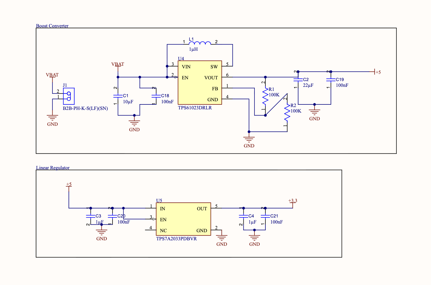
The power architecture generates a 5 V rail with a switching regulator, then derives 3.3 V through a linear regulator. Separate rails let the RF / analog and digital sections receive the voltages required by their selected components.
MCU, communication, and debug
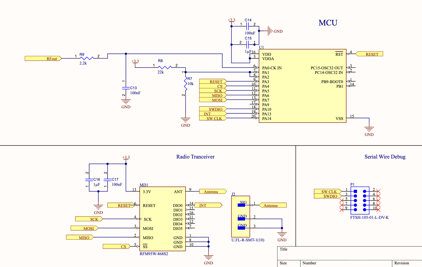
The MCU receives the detector's low-frequency analog output and provides a path for basic processing or communication of detection information. A separate radio module and U.FL connection support wireless communication, while an SWD header provides programming and debug access.
PCB integration
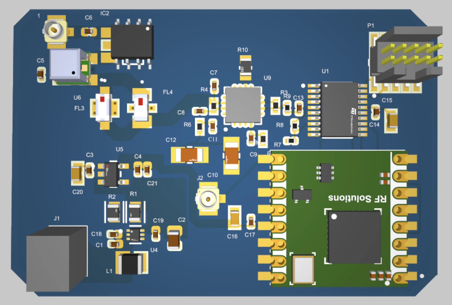
The board brings the RF input, gain stage, filters, logarithmic detector, MCU, auxiliary wireless module, power supplies, and programming interface into one layout.
Component placement reflects an attempt to keep the RF path relatively direct and to place it away from switching power and digital circuitry where practical. It should be read as a first RF-layout iteration rather than a production-optimized or impedance-verified board.
- RF input and front-end circuitry
- Mini-Circuits RF filters
- AD8318 logarithmic detector
- MCU and analog detector input
- Auxiliary wireless module
- 5 V / 3.3 V power supplies
- Programming and debug interface
Engineering lessons
- 01
Controlled-impedance routing
My first practical exposure to laying out traces around a target characteristic impedance instead of treating them as ideal wires.
- 02
RF return paths
Learned why a close, uninterrupted ground reference is critical to the behaviour of a high-frequency interconnect.
- 03
Physical placement
At GHz frequencies, routing distance, pads, connectors, and component placement become meaningful circuit parameters.
- 04
Logarithmic RF detection
Learned how a log detector compresses a wide RF input range into an analog signal that a conventional MCU can measure.
- 05
Filtering before detection
Learned why selectivity has to occur ahead of a broadband detector when the architecture needs sensitivity to particular frequency regions.
- 06
Power integrity
Gained a better appreciation for local decoupling and for separating noisy switching circuitry from sensitive analog and RF paths.
This project was an introduction to RF PCB design rather than a complete RF engineering exercise. It showed me how much additional characterization—such as VNA measurements, gain and loss measurements, detector calibration, and real-world RF testing—would be required to turn the concept into a robust receiver.