Overview
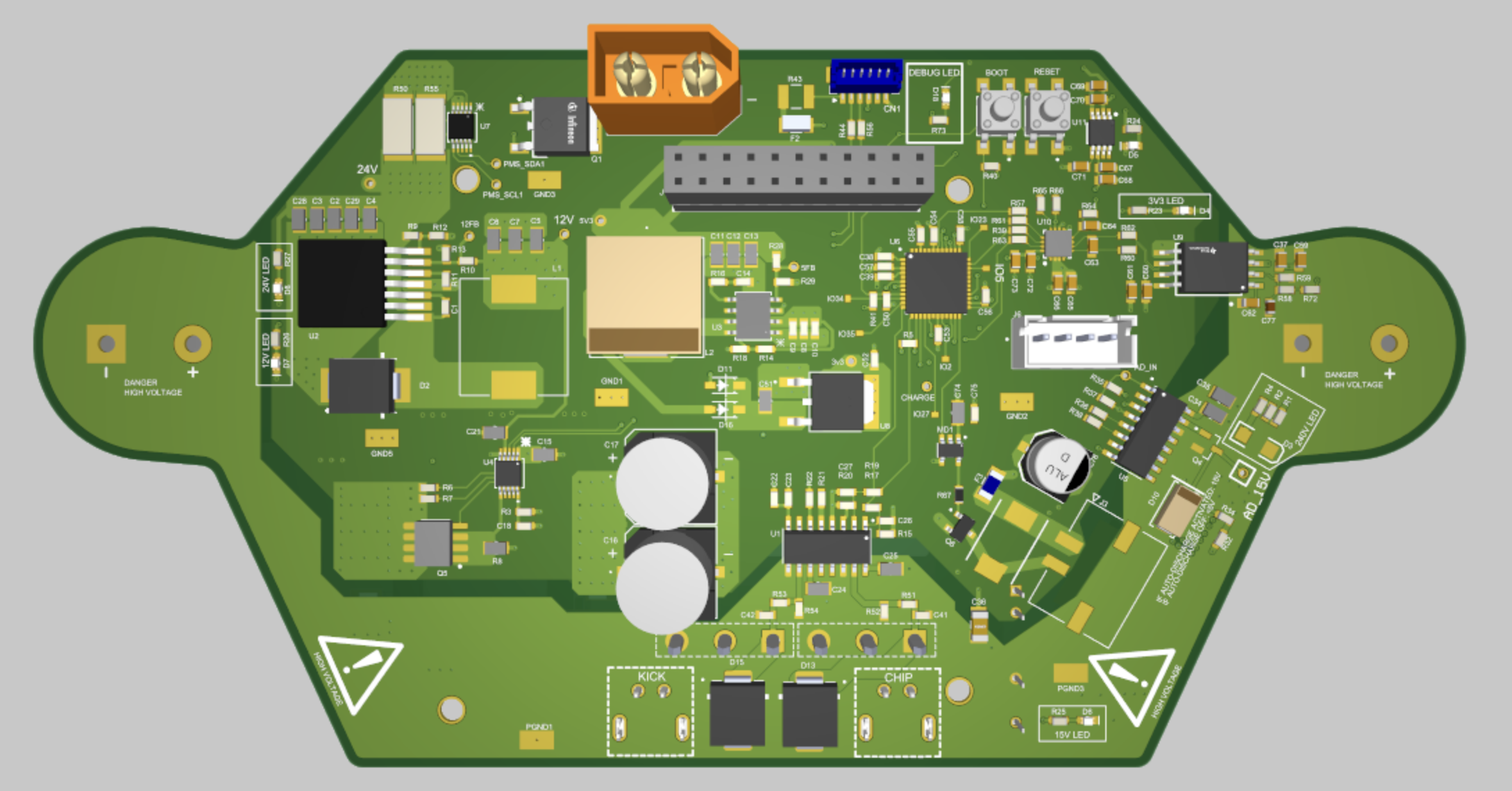
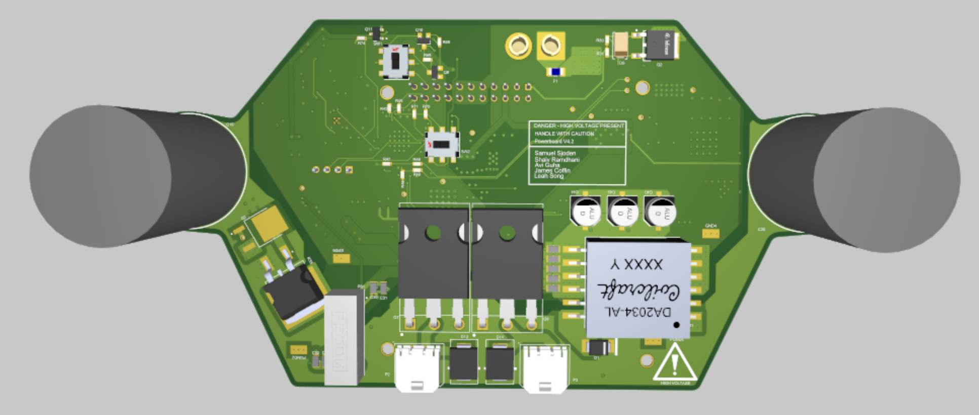
Redesigned the power distribution and high-voltage board for UBC Thunderbots, an autonomous soccer-playing robot team. The board takes in power from a 24 V battery and generates several regulated rails, including 12 V, 5.3 V, 3.3 V, an isolated 15 V rail, and a high-voltage 240 V rail.
The 240 V rail is generated using a flyback converter and is used to charge capacitors for the robot’s kick and chip mechanisms. The redesign focused on improving the PCB layout, maintaining galvanic isolation between high-voltage and low-voltage domains, adding new functionality, and making the board easier to test and debug.
Board renders
Front view
Back view
Problem
The existing power board needed to be updated because of both electrical and mechanical constraints. Some switching converters, especially the flyback converter, had noise concerns that motivated a layout-focused redesign. The board also needed to accommodate updated connector locations due to mechanical changes in the robot.
In addition, the previous revision had limited access to important test nodes, making debugging more difficult. New functionality also needed to be added, including high-voltage feedback, a dribbler motor driver circuit, and auto-flashing circuitry for firmware deployment.
Constraints
The board had to operate from the robot’s 24 V battery system while generating multiple isolated and non-isolated rails:
- 12 V and 5.3 V using buck converters
- 3.3 V using an LDO
- 15 V using an isolated DC/DC converter for the high-voltage domain
- 240 V using a flyback converter for charging kick/chip capacitors
The PCB used a four-layer stackup with signal, power, ground, and signal layers. The power and ground regions were split between high-voltage and low-voltage domains to preserve galvanic isolation. The design also had to fit within the robot’s mechanical constraints, support existing communication interfaces, and be testable during a fast prototype-to-final-board timeline.
My contribution
I worked on the layout-focused redesign of the power board and integrated several new schematic blocks into the prototype revision.
My contributions included:
- Reworking PCB layout to improve converter placement, routing, and mechanical integration
- Adding a high-voltage feedback circuit using an isolated amplifier
- Adding a dribbler motor driver circuit using isolated gate drivers
- Adding USB-to-UART auto-flashing circuitry for firmware deployment
- Rerouting connectors to match updated mechanical constraints
- Adding test points to improve access to flyback, buck converter, and other critical nets
- Routing UART, I2C, and SPI interfaces across the board
- Planning validation steps for flyback testing, high-voltage feedback, and ground isolation checks
Technical decisions
The design used galvanic isolation to separate the low-voltage control electronics from the high-voltage capacitor-charging system. Isolation was implemented through the flyback transformer, an isolated 12 V to 15 V DC/DC converter, isolated gate drivers, and an isolated amplifier for high-voltage sensing.
The flyback converter was a major layout focus because it generates the 240 V rail used to charge the kick and chip capacitors. The redesign emphasized reducing high-current loop area, improving placement around switching nodes, and preparing for future characterization of primary-side noise and possible snubber changes.
The board also used multiple communication protocols depending on subsystem needs. UART was used for flashing and debugging, I2C was used for power monitoring, and SPI was used for high-voltage sensing. Additional headers and test points were added to make the board easier to probe and modify during bring-up.
A prototype-first strategy was used: rather than completely redesigning the full board immediately, the existing layout was reused where practical while new circuits and test features were added. This allowed the team to validate the new functionality before committing to the final revision.
Results
The redesign produced a prototype-ready version of the power board with improved layout, added high-voltage feedback, dribbler motor driver circuitry, auto-flashing support, and better test access.
The most important outcome was making the board easier to validate and iterate on. The added test points and debug access allow future testing of the flyback converter, buck converters, high-voltage feedback circuit, and isolation strategy.
This project taught me how strongly PCB layout affects switching power supply performance, especially in high-voltage flyback converters. It also gave me experience thinking about galvanic isolation, mixed-voltage PCB layout, power distribution, and designing hardware for testability rather than only for functionality.